
Machine vision sensors should be selected according to the application they are to be used for. The two scanning types of sensors are line and area scanners, where the former is more demanding. The “area” refers to the sensor shape inside the camera. The line-scanning sensor provides a one-dimensional line at a time, whereas the area-scanning sensor produces two-dimensional data. Therefore, the area scanner is a typical choice for general applications.
The two main types of sensors are charge-coupled devices (CCD) and complementary metal oxide semiconductors (CMOS). The main difference between the sensor types is the pixel-level conversion from charge to voltage. CCD uses sequential methods, whereas the CMOS sensor reads the pixels parallel. Currently, the performance of CMOS sensors has exceeded CDDs, and CMOS sensors are widely used in machine vision applications.
With CMOS sensors, each pixel is addressable on a row and column basis. The voltages are read parallel, enabling high frame rates and users to define the regions of interest (ROIs). Depending on the number of transistors per pixel, the sensor might have a global shutter or a higher signal-to-noise ratio. The sensor’s pixel-level operating principles and basic characteristics are described in the following subsections. Next, we will see the basic principles of an imaging sensor: how the photons are converted to digital numbers.
2.2.1 A simplified physical model of a pixel and imaging sensor
The pixel’s function is to convert the incoming photons into electrons. The electrons are converted into a voltage, which can be measured. Each sensor has a full-well capacity, which describes the maximum number of electrons stored in a pixel. Below, Figure 1 illustrates a pixel well and a physical model of an imaging sensor that converts the photons into digital numbers. As can be seen in Figure 1, the full-well area is proportional to the pixel’s light-sensitive front area.
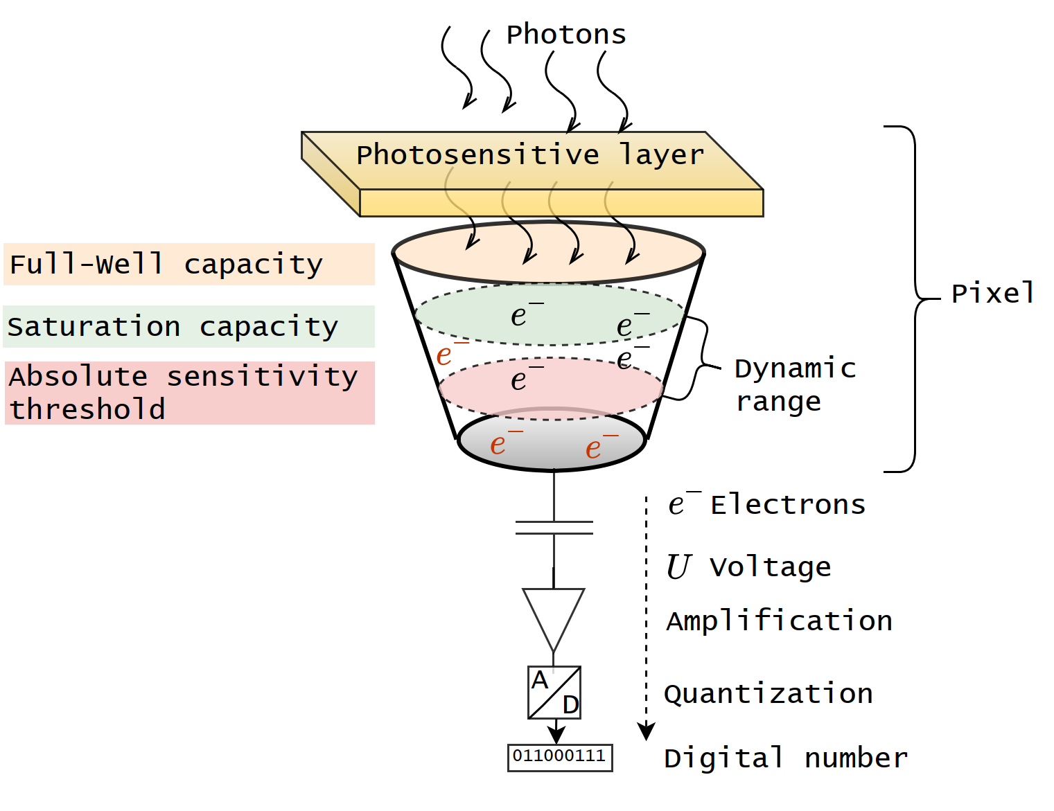
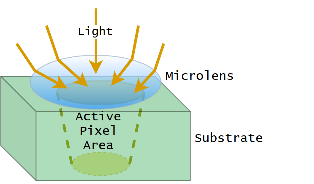
Dynamic range (DR, Figure 1) is the ratio between the smallest and largest amplitude of the signal a sensor can produce (Baumer 2022). It describes the imager’s ability to simultaneously provide detailed information from bright and dark areas. The parameter is important when the illumination conditions rapidly change or the targets have a strong contrast. The area that can capture light is called the fill factor. Since each pixel in a CMOS sensor has its own readout, charge conversion and digitalisation structures (visualised as the substrate, below in Figure 9), the interline transfer might have a 20-50% fill factor from the pixel size (Stemmer 2022). This affects the sensors’ overall photosensitivity, which can be improved, for instance, by using microlenses in front of the pixels (Figure 2).
Photons are converted into electrons, and the conversion ratio is called quantum efficiency (QE). The quantum efficiency depends on the wavelength. The sensor’s light sensitivity depends on the number of photons converted to electrons. The more photons are converted, the greater the quantum efficiency, increasing the level of information provided by the sensor. If the sensor is used with filters, the measured quantum efficiency of the system might differ from the sensor-level quantum efficiency (EMVA 2016).
Found something useful? Wish to cite? This post is based on my dissertation. For citations and more information, click here to see the scientific version of it.
References
Baumer 2022. Baumer Group, Operating principles of CMOS sensors. URL:https://www.baumer.com/es/en/service-support/function-principle/operating-principle-and-features-of-cmos-sensors/a/EMVA1288. (A leading manufacturer of sensors, encoders, measuring instruments and components for automated image-processing. Accessed on 7.4.2022).
Stemmer 2022. Stemmer Imaging, The Imaging and Vision Handbook. ⟨URL:https://www.stemmer-imaging.com/en/the-imaging-vision-handbook/⟩. (A leading international machine vision technology provider. Accessed on 7.4.2022).
EMVA 2016. The European machine vision association, EMVA Standard 1288, Release 3.1. https://www.emva.org/standards-technology/emva-1288/emva-standard-1288-downloads-2/⟩. (Sensor and camera standards. Accessed on 8.4.2022).