When the sensor is mounted with optical elements, such as lenses and other optomechanical components, we can call it a machine vision camera or machine vision imager. Machine vision cameras require optical design.
Commercial lenses can be used with optomechanical components and machine vision sensors. Further, prototype imagers can be built from scratch using, for example, extension tubes, individual lenses and filters.
Combining a sensor and lens requires only a basic understanding of an imager’s design, whereas the more complex systems require a mathematical understanding of the geometrical optics. Both approaches can be valuable in science and enineering. Prototypes pave the way for new applications, and the optics, if needed, can be improved within the continuation studies and tests.
This series of posts introduces the basic terminology for optics, which would help to select and understand the optical parameters for designing a machine vision imager.
At first, we will get known with optics’ terminology (Post 3.1); next, within Post 3.2, we will form an optical image. Post 3.3 introduces lens mounts, 3.4 explains the image circle and sensor diagonal details. Focal length, magnification and working distance are covered in Post 3.5, and the series of posts is finalised with a peek of optical and optomechanical components (Post 3.6).
After reading 2.2, we now understand the operating principles. Let’s deepen the understanding by discussing some important sensor properties and getting to know with Bayer pattern.
Sensor noise and signal-to-noise ratio
Sensors have different sources of noise. Dark current noise occurs when the electrons emerge through thermal processes in the pixel. The level is related to temperature and exposure time by increasing with them. Photon noise is caused by light, as the photon flux striking the sensor is Poisson-distributed (EMVA 2016). This limits the maximum signal-to-noise ratio (SNR). Readout noise occurs when the electrons are converted into voltages. The quantisation noise is caused when the voltages with continuous values are converted to digital values with discrete values (A/D-conversion). Temporal noise is a combination of all the aforementioned sources of noise. It exists even when the pixels are not illuminated. The exposure time and temperature generate electrons without light. The level of a dark signal varies.
The signal-to-noise ratio is the ratio between the maximum signal and the noise floor. It describes a real signal after the A/D conversion. When the signal-to-noise ratio is 1, the maximum signal and noise floor levels are equal (EMVA (2016) and Stemmer (2022)).
Sensor sensitivity and spectral response
The quantum efficiency and background noise influence the sensitivity of the sensor. The sensitivity is high when the quantum efficiency is high and the background noise level is low. The background noise level is measured with the lens covered. Each pixel has an absolute sensitivity threshold (AST), which describes the lowest possible number of photons with which the sensor can produce a useful image. The sensitivity of a sensor increases when the threshold decreases. The absolute sensitivity threshold is a significant variable in low-light applications. Absolute sensitivity threshold combines the quantum efficiency, dark noise and shot noise values and it is determined when the signal-to-noise ratio level is 1 (EMVA (2016); Stemmer (2022) and Baumer (2022)).
Spectral response describes the wavelength range that a sensor can capture. Typically, the CMOS sensor’s range is from 350 nm to 1100 nm (EMVA 2016). Some CMOS sensors might have enhanced sensitivities for VNIR imaging at the range of 700 – 1000nm. The spectral imagers used for IR applications can use InGaAs sensors that have a range of 900 to 1700 nm or SWIR sensors. The UV sensors’ spectral sensitivity ranges upwards from 200 nm (EMVA 2016).
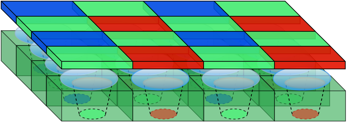
The number of active pixels in a sensor is called spatial resolution. The optimum resolution should be calculated target-wisely for robust inspection systems. The key is to use the measures of the smallest feature in the field of view, which defines the minimum resolution. As a practical example, suppose the feature size is 1 × 1, the object size is 100 × 100, and the analysis method requires 3 × 3 pixels per one feature. The minimum resolution is addressed by multiplying the object size with the requirement: 300 × 300 pixels (Stemmer 2022). The mentioned formula is for monochromatic sensors. The minimum resolution for a colour sensor with a Bayer pattern should be doubled. (What is a Bayer pattern, see figure 1)
Spatial resolution and shutter types
The sensor shutter type describes how the sensor exposes the pixels. A rolling shutter starts and stops the exposure sequentially, row-by-row or pixel-wise. The delay of all pixels to be exposed can be up to 1/framerate, which can be an issue when the target moves (Stemmer 2022). A rolling shutter sensor might have a global shutter start, which allows all pixels to be activated for exposure simultaneously but turned off sequentially. This mode might cause some blurring to the bottom areas of the image, and its use demands a proper illumination design. The global shutter activates and deactivates its pixels at once, being the most practical choice in most applications dealing with moving targets.
Monochromatic and colour sensors and Bayer pattern
Sensors can be divided into monochromatic and colour sensors, and the selection should be made depending on the target. The main difference between monochromatic and colour sensors is the colour filter placed in front of the pixels. A sensor with a pixel-wise filter provides colour filter arrays (CFAs) that can be computed to colour images using demosaic algorithms. In contrast, the monochromatic sensor provides data that can be processed as an image directly.
The CFA limits the sensitivity of each receiving pixel well into a single part of the visible spectrum. Therefore, each red-green-blue (RGB) channel’s CFA pixel has a limited spectral range, representing either red, green or blue spectral responses (Alleysson et al. 2003). The CFA filter is part of the imaging system’s spectral sensitivity, which is determined as a combination of the sensor sensitivity and the transmittance of the CFA filter, such as Bayer blue-green-green-red (BGGR) (Sadeghipoor et al. 2012).
Figure 1. The Bayer BGGR pattern filter is placed in front of the sensor’s photosensitive pixel wells. The pixel wells measure the intensity of light, providing information to green, blue or red pixels. The full three-channel RGB image is produced with interpolation for the missing pixel values.
Above, Figure 1 visualises the Bayer pattern BGGR filter placed in front of the sensor. Bayer BGGR filter is a common RGB filter, repeating patterns of 2 × 2 pixels: one blue, two green and one red. Demosaic algorithms perform an interpolation that estimates the three-pixel values of the RGB image Eskelinen (2019).
Eskelinen, M. 2019. Computational methods for hyperspectral imaging using Fabry-Perot interferometers and colour cameras. URL:http://urn.fi/URN:ISBN:978-951-39-7967-6.
Sadeghipoor, Z., Lu, Y. M. & Süsstrunk, S. 2012. Optimum spectral sensitivity functions for single sensor color imaging. In Digital photography VIII, Vol. SPIE, 26–39. doi:https://doi.org/10.1117/12.907904.
More information
Baumer 2022. Baumer Group, Operating principles of CMOS sensors. URL:https://www.baumer.com/es/en/service-support/function-principle/operating-principle-and-features-of-cmos-sensors/a/EMVA1288. (A leading manufacturer of sensors, encoders, measuring instruments and components for automated image-processing. Accessed on 7.4.2022).
EMVA 2016. The European machine vision association, EMVA Standard 1288, Release 3.1. https://www.emva.org/standards-technology/emva-1288/emva-standard-1288-downloads-2/⟩. (Sensor and camera standards. Accessed on 8.4.2022).
Stemmer 2022. Stemmer Imaging, The Imaging and Vision Handbook. ⟨URL:https://www.stemmer-imaging.com/en/the-imaging-vision-handbook/⟩. (A leading international machine vision technology provider. Accessed on 7.4.2022).
Machine vision sensors should be selected according to the application they are to be used for. The two scanning types of sensors are line and area scanners, where the former is more demanding. The “area” refers to the sensor shape inside the camera. The line-scanning sensor provides a one-dimensional line at a time, whereas the area-scanning sensor produces two-dimensional data. Therefore, the area scanner is a typical choice for general applications.
The two main types of sensors are charge-coupled devices (CCD) and complementary metal oxide semiconductors (CMOS). The main difference between the sensor types is the pixel-level conversion from charge to voltage. CCD uses sequential methods, whereas the CMOS sensor reads the pixels parallel. Currently, the performance of CMOS sensors has exceeded CDDs, and CMOS sensors are widely used in machine vision applications.
With CMOS sensors, each pixel is addressable on a row and column basis. The voltages are read parallel, enabling high frame rates and users to define the regions of interest (ROIs). Depending on the number of transistors per pixel, the sensor might have a global shutter or a higher signal-to-noise ratio. The sensor’s pixel-level operating principles and basic characteristics are described in the following subsections. Next, we will see the basic principles of an imaging sensor: how the photons are converted to digital numbers.
2.2.1 A simplified physical model of a pixel and imaging sensor
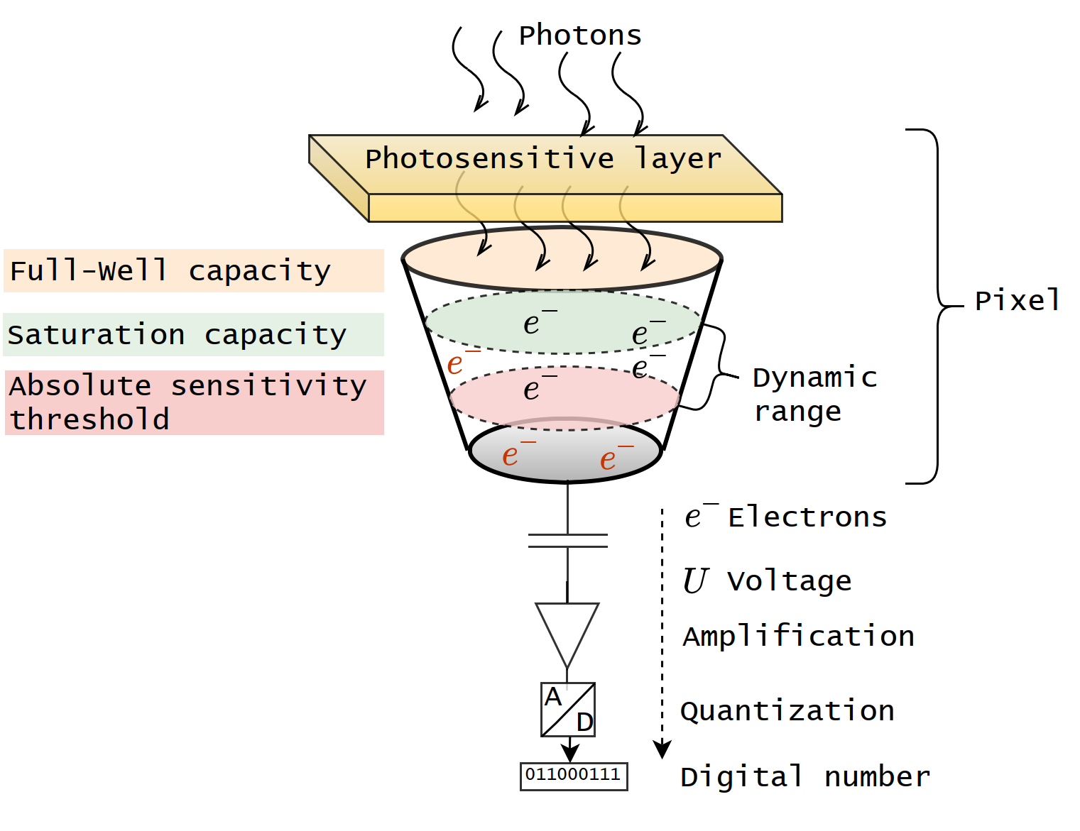
The pixel’s function is to convert the incoming photons into electrons. The electrons are converted into a voltage, which can be measured. Each sensor has a full-well capacity, which describes the maximum number of electrons stored in a pixel. Below, Figure 1 illustrates a pixel well and a physical model of an imaging sensor that converts the photons into digital numbers. As can be seen in Figure 1, the full-well area is proportional to the pixel’s light-sensitive front area.
Figure 1. A simplified physical model of a pixel and imaging sensor. A number of photons hit the photosensitive pixel area during the exposure time. The photons are converted to photo-electrons. The charge formed by the electrons e− is then converted by a capacitor to a voltage, before being amplified and digitised, resulting in the digital grey values. The red e− denotes temporal noise. The pixel-depth dependent physical properties, from the full-well capacity to the dynamic range, are visualised in the pixel well.
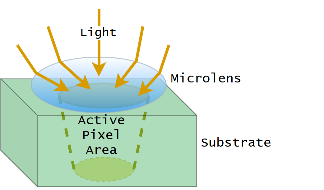
Dynamic range (DR, Figure 1) is the ratio between the smallest and largest amplitude of the signal a sensor can produce (Baumer 2022). It describes the imager’s ability to simultaneously provide detailed information from bright and dark areas. The parameter is important when the illumination conditions rapidly change or the targets have a strong contrast. The area that can capture light is called the fill factor. Since each pixel in a CMOS sensor has its own readout, charge conversion and digitalisation structures (visualised as the substrate, below in Figure 9), the interline transfer might have a 20-50% fill factor from the pixel size (Stemmer 2022). This affects the sensors’ overall photosensitivity, which can be improved, for instance, by using microlenses in front of the pixels (Figure 2).
Figure 2. Full well capacity i.e., the maximum electrical charge possible, is limited by the physical pixel depth. One way to improve the pixel’s photosensitivity is to use microlenses above the pixel well. Therefore, some of the light heading into the sensor’s substrate areas can be directed to the pixel.
Photons are converted into electrons, and the conversion ratio is called quantum efficiency (QE). The quantum efficiency depends on the wavelength. The sensor’s light sensitivity depends on the number of photons converted to electrons. The more photons are converted, the greater the quantum efficiency, increasing the level of information provided by the sensor. If the sensor is used with filters, the measured quantum efficiency of the system might differ from the sensor-level quantum efficiency (EMVA 2016).
Baumer 2022. Baumer Group, Operating principles of CMOS sensors. URL:https://www.baumer.com/es/en/service-support/function-principle/operating-principle-and-features-of-cmos-sensors/a/EMVA1288. (A leading manufacturer of sensors, encoders, measuring instruments and components for automated image-processing. Accessed on 7.4.2022).
Stemmer 2022. Stemmer Imaging, The Imaging and Vision Handbook. ⟨URL:https://www.stemmer-imaging.com/en/the-imaging-vision-handbook/⟩. (A leading international machine vision technology provider. Accessed on 7.4.2022).
EMVA 2016. The European machine vision association, EMVA Standard 1288, Release 3.1. https://www.emva.org/standards-technology/emva-1288/emva-standard-1288-downloads-2/⟩. (Sensor and camera standards. Accessed on 8.4.2022).
Two important standards are briefly introduced in this section, hosted by the European machine vision associate (EMVA), a non-profit organisation founded in 2003. The EMVA aims to connect organisations in machine vision, computer vision, embedded vision and imaging technologies, which includes manufacturers, system and machine builders, integrators, distributors, consultancies, research organisations and academia (EMVA 2022).
The reason for introducing these standards is that a standard might be valuable for comparing different sensors and it may enable a more versatile programming interface than a common programming library.
The first standard is EMVA 1288, which can be used for comparing sensors; the second standard is GenICam, which provides a generic programming interface for sensors and other devices.
When comes to authors’ hands-on experience, the GenICam standard is the foundation of the Python library Camazing (Jääskeläinen et al. 2019a), which is used with VTTs HS imagers, which are mentioned also in my posts. Camazing was developed at the Spectral Imaging Laboratory at the University of Jyväskylä (JYU 2022) with an MIT license.
EMVA 1288
Sensor selection is the first phase, and one of the most important ones in the image-capturing process. Manufacturers offer a large selection of different sensors, which vary in their price. Some of the properties introduced in the Post 2.2 are definably dependent on the requirements of the target; such as the resolution, the choice between monochromatic or colour sensor, the shutter type and the camera interface. The challenge lies in the measurable features; such as the sensor’s sensitivity, temporal noise and spectral response.
EMVA 1288 is a standard for the specification and measurement of machine vision sensors and cameras (EMVA 2022). Its main purpose is to create transparency by defining reliable and exact measurement procedures and data presentation guidelines to make comparing cameras and image sensors easier.
Manufacturers that do not hold EMVA licences might measure and present the sensor performance and feature measurements differently and may even leave some important details to the buyers to test, which might be expensive and difficult.
Manufacturers that adhere to the EMVA 1288 standard measure the sensors and cameras according to the standard’s exact measurement procedures, making the presented data sheets of different sensors and sensor manufacturers comparable. The “EMVA standard 1288 compliant” logo ensures that products are licensed, measured and presented transparently and reliably.
The complete list of measurement groups and their mandatorily can be found in the standard specification (EMVA 2016). The standard’s documentation includes mathematical formulas, descriptions of the measurement setups and guidelines for presenting the results in a consistent format. The current release cited in this Post is 3.1.
GenICam standard
Generic Interface for Cameras (GenICamTM) provides a generic programming interface for various sensors, cameras and other devices, regardless of the interface technology (GigE Vision, USB3 Vision, CoaXPress, Camera Link HS, Camera Link, etc.) they use or what the features they implement.
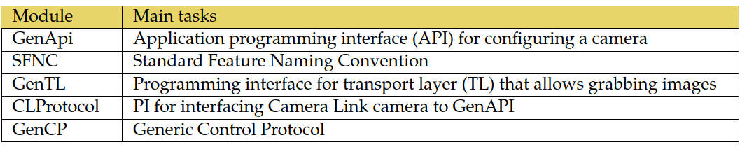
Table 1. The GenICam standard modules (GenICam 2022).
The GenICam standard comprises five modules, which are introduced above in Table 4. The role of GenApi is to define the mechanism used to provide the generic application defining interface (API) via a self-describing eXtensible Markup Language (XML) file in the device. The XML file format is defined in Schema, which is a part of GenApi. Underneath GenApi is the standard features naming convention (SFNC), which standardises the name, type, meaning and use of device features, resulting in standard functionalities between manufacturers. The features are typically introduced in a tree view, being controllable via an application. The related standard for the consistent naming of pixel formats is the pixel format naming convention (PFNC).
GenTL is the standard for the transport layer programming interface. As a low-level API, it provides standard device interfaces and allows one to enumerate devices, access device registers, stream data and deliver asynchronous events. Data Container (GenDC) module allows devices to send any form of data (e.g. 1D, 2D, 3D, multi-spectral, metadata) in a Transport Layer Protocol (TLP) independent format and permits to share of a common data container format for all the TLP standards. The control protocol (GenCP) is a low-level standard to define the packet format for device control and can be used as a control protocol for each new standard.
The main purpose and benefit of GenICam are to provide an API, which is identical regardless of interface technology used in standardised devices (GenICam 2022).
GenICam 2022. The European machine vision association, GenICam standard, version 2.1.1. https://www.emva.org/standards-technology/genicam/ introduction-new/
EMVA 2022. The European machine vision association, home page. https: /www.emva.org/. (Organisation behind sensor and camera standards. Accessed on 8.4.2022).
Jääskeläinen, S., Eskelinen, M., Annala, L. & Raita-Hakola, A.-M. 2019a. Camazing Python library. https://pypi.org/project/camazing/. (Machine vision library for GenICam-compliant cameras. Developed at the University of Jäskylä, Spectral Imaging Laboratory. Released under MIT-licence. Accessed on 9.4.2022).