PhD in computer science, MBA in entrepreneurship and business competence
Anna-Maria Raita-Hakola
Anna-Maria defended her dissertation in December 2022. At the same time, she finalised her five-year-long journey of deepening her skills into a new career. Her computer science master studies started in January 2017 when she wrote her “Hello world” in C#, with no previous experience in programming.
Before her career change, she has been working in the business field, including versatile tasks in marketing, productizing, sales, accounting, customer service, business management, and HR. She has collected approximately 8 to 10 years experience of in leadership (maternity leaves affect the number of years). During her years as a team leader, she participated in several management and leadership programs provided by the companies she worked for. The work experience arises from SMEs, listed companies and the public domain (the Social Insurance Institution (SII)).
Currently, she is a PhD in computer science, with a wide experience and skills from sensor-level programming to data processing and analysis. During her studies, she was lucky to be hired to the Spectral imaging laboratory, where she has been working for nearly five years.
She started as a software developer, and she is the main author of the CubeView software, which is software for hyperspectral imaging and analysis for VTTs prototype imagers. She is capable of designing and implementing machine vision systems, from the device workflows enabling scientific spectral data gathering with customised user interfaces.
The gathered work experience during her master’s studies related heavily to designing and implementing device-controlling phases for machine vision sensors and optical components and user interface developing tasks.
After she graduated (MSc), she focused on computational data analysis, achieving Aaltonen Säätiö grant. She has been developing three new machine learning methods (New versions of Minimal Learning Machine, MLM, see Nokia awards 2022) and skin cancer research from hyperspectral (HS) images, using data that is captured with the CubeView Hospital imaging system, which she developed.
The skin cancer research was conducted using convolutional neural networks and 3D HS imaging. During her doctoral studies, she worked as a part-time machine vision engineer at Solteq Robotics (see the award-winning retail robot).
Currently, she continues her research in the field of computational data science (wildfire detection and prediction, FireMan project). She is a teacher of machine learning, anomaly detection and machine vision courses at the University of Jyväskylä. She is building a machine vision laboratory, a concept that allows students to get hands-on with machine vision sensors and Raspberry Pi cameras. She works as a supervisor for two master’s students and two research assistants and begins supervising a graduate student this spring. She enjoys teaching and actively tests and develops methods that are close to leadership methods, allowing the students to be active, and see and understand the meaning of the subjects related to their career dreams.
When the sensor is mounted with optical elements, such as lenses and other optomechanical components, we can call it a machine vision camera or machine vision imager. Machine vision cameras require optical design.
Commercial lenses can be used with optomechanical components and machine vision sensors. Further, prototype imagers can be built from scratch using, for example, extension tubes, individual lenses and filters.
Combining a sensor and lens requires only a basic understanding of an imager’s design, whereas the more complex systems require a mathematical understanding of the geometrical optics. Both approaches can be valuable in science and enineering. Prototypes pave the way for new applications, and the optics, if needed, can be improved within the continuation studies and tests.
This series of posts introduces the basic terminology for optics, which would help to select and understand the optical parameters for designing a machine vision imager.
At first, we will get known with optics’ terminology (Post 3.1); next, within Post 3.2, we will form an optical image. Post 3.3 introduces lens mounts, 3.4 explains the image circle and sensor diagonal details. Focal length, magnification and working distance are covered in Post 3.5, and the series of posts is finalised with a peek of optical and optomechanical components (Post 3.6).
Welcome to araita.com. This website is a place to read and learn the whole scale, from sensors to machine vision systems and analysis (AI). We will learn basic terminology, operating principles and more from machine vision sensors, optics, optical components, programming, data acquisition, image transformation and analysis using machine learning methods.
Since the author is currently working as a scientist, araita.com is based on academics and science, and therefore it contains material from her publications and dissertation. The visualisations and materials are here for citations (the origin is mentioned in every post) and re-use but by following academic conventions.
Besides the machine vision, machine learning, and hyperspectral imaging materials, araita.com contains the author’s teaching portfolio, publication details and a series of posts related to management, leadership and communication, which is raised from her MBA education.
You will find the educational materials From sensors to analysis materials under the “content” menu or from the right sidebar.
After reading 2.2, we now understand the operating principles. Let’s deepen the understanding by discussing some important sensor properties and getting to know with Bayer pattern.
Sensor noise and signal-to-noise ratio
Sensors have different sources of noise. Dark current noise occurs when the electrons emerge through thermal processes in the pixel. The level is related to temperature and exposure time by increasing with them. Photon noise is caused by light, as the photon flux striking the sensor is Poisson-distributed (EMVA 2016). This limits the maximum signal-to-noise ratio (SNR). Readout noise occurs when the electrons are converted into voltages. The quantisation noise is caused when the voltages with continuous values are converted to digital values with discrete values (A/D-conversion). Temporal noise is a combination of all the aforementioned sources of noise. It exists even when the pixels are not illuminated. The exposure time and temperature generate electrons without light. The level of a dark signal varies.
The signal-to-noise ratio is the ratio between the maximum signal and the noise floor. It describes a real signal after the A/D conversion. When the signal-to-noise ratio is 1, the maximum signal and noise floor levels are equal (EMVA (2016) and Stemmer (2022)).
Sensor sensitivity and spectral response
The quantum efficiency and background noise influence the sensitivity of the sensor. The sensitivity is high when the quantum efficiency is high and the background noise level is low. The background noise level is measured with the lens covered. Each pixel has an absolute sensitivity threshold (AST), which describes the lowest possible number of photons with which the sensor can produce a useful image. The sensitivity of a sensor increases when the threshold decreases. The absolute sensitivity threshold is a significant variable in low-light applications. Absolute sensitivity threshold combines the quantum efficiency, dark noise and shot noise values and it is determined when the signal-to-noise ratio level is 1 (EMVA (2016); Stemmer (2022) and Baumer (2022)).
Spectral response describes the wavelength range that a sensor can capture. Typically, the CMOS sensor’s range is from 350 nm to 1100 nm (EMVA 2016). Some CMOS sensors might have enhanced sensitivities for VNIR imaging at the range of 700 – 1000nm. The spectral imagers used for IR applications can use InGaAs sensors that have a range of 900 to 1700 nm or SWIR sensors. The UV sensors’ spectral sensitivity ranges upwards from 200 nm (EMVA 2016).
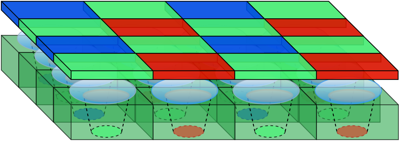
The number of active pixels in a sensor is called spatial resolution. The optimum resolution should be calculated target-wisely for robust inspection systems. The key is to use the measures of the smallest feature in the field of view, which defines the minimum resolution. As a practical example, suppose the feature size is 1 × 1, the object size is 100 × 100, and the analysis method requires 3 × 3 pixels per one feature. The minimum resolution is addressed by multiplying the object size with the requirement: 300 × 300 pixels (Stemmer 2022). The mentioned formula is for monochromatic sensors. The minimum resolution for a colour sensor with a Bayer pattern should be doubled. (What is a Bayer pattern, see figure 1)
Spatial resolution and shutter types
The sensor shutter type describes how the sensor exposes the pixels. A rolling shutter starts and stops the exposure sequentially, row-by-row or pixel-wise. The delay of all pixels to be exposed can be up to 1/framerate, which can be an issue when the target moves (Stemmer 2022). A rolling shutter sensor might have a global shutter start, which allows all pixels to be activated for exposure simultaneously but turned off sequentially. This mode might cause some blurring to the bottom areas of the image, and its use demands a proper illumination design. The global shutter activates and deactivates its pixels at once, being the most practical choice in most applications dealing with moving targets.
Monochromatic and colour sensors and Bayer pattern
Sensors can be divided into monochromatic and colour sensors, and the selection should be made depending on the target. The main difference between monochromatic and colour sensors is the colour filter placed in front of the pixels. A sensor with a pixel-wise filter provides colour filter arrays (CFAs) that can be computed to colour images using demosaic algorithms. In contrast, the monochromatic sensor provides data that can be processed as an image directly.
The CFA limits the sensitivity of each receiving pixel well into a single part of the visible spectrum. Therefore, each red-green-blue (RGB) channel’s CFA pixel has a limited spectral range, representing either red, green or blue spectral responses (Alleysson et al. 2003). The CFA filter is part of the imaging system’s spectral sensitivity, which is determined as a combination of the sensor sensitivity and the transmittance of the CFA filter, such as Bayer blue-green-green-red (BGGR) (Sadeghipoor et al. 2012).
Figure 1. The Bayer BGGR pattern filter is placed in front of the sensor’s photosensitive pixel wells. The pixel wells measure the intensity of light, providing information to green, blue or red pixels. The full three-channel RGB image is produced with interpolation for the missing pixel values.
Above, Figure 1 visualises the Bayer pattern BGGR filter placed in front of the sensor. Bayer BGGR filter is a common RGB filter, repeating patterns of 2 × 2 pixels: one blue, two green and one red. Demosaic algorithms perform an interpolation that estimates the three-pixel values of the RGB image Eskelinen (2019).
Eskelinen, M. 2019. Computational methods for hyperspectral imaging using Fabry-Perot interferometers and colour cameras. URL:http://urn.fi/URN:ISBN:978-951-39-7967-6.
Sadeghipoor, Z., Lu, Y. M. & Süsstrunk, S. 2012. Optimum spectral sensitivity functions for single sensor color imaging. In Digital photography VIII, Vol. SPIE, 26–39. doi:https://doi.org/10.1117/12.907904.
More information
Baumer 2022. Baumer Group, Operating principles of CMOS sensors. URL:https://www.baumer.com/es/en/service-support/function-principle/operating-principle-and-features-of-cmos-sensors/a/EMVA1288. (A leading manufacturer of sensors, encoders, measuring instruments and components for automated image-processing. Accessed on 7.4.2022).
EMVA 2016. The European machine vision association, EMVA Standard 1288, Release 3.1. https://www.emva.org/standards-technology/emva-1288/emva-standard-1288-downloads-2/⟩. (Sensor and camera standards. Accessed on 8.4.2022).
Stemmer 2022. Stemmer Imaging, The Imaging and Vision Handbook. ⟨URL:https://www.stemmer-imaging.com/en/the-imaging-vision-handbook/⟩. (A leading international machine vision technology provider. Accessed on 7.4.2022).